Clean Electronics with Boron Solutions
Technology has forever been a part of our lives. It brings both good and bad things to the world; it allows us to access information and enables society as we know it today with cell phones, computers, internet connections, and more.
The noise from an electronic device is never-ending for those who are constantly in contact or near these devices daily; however, this may be why many people do their best work at home where there are fewer distractions such as TV soundtracks that can keep them up late into the night when they should be sleeping instead of working hard towards achieving professional goals.
When we think about the future today, we think about technology and how it will change everything we know. Computer scientists are working hard at developing faster processors and creating more applications in every field we can think about. Boron and Electronics are at the heart of good engineering technology, but the solutions that may work for us today may not be enough for tomorrow’s technology. Let’s see how technology can benefit from Boron.
Ion implantation
The process of implanting ions into a solid material is known as ion implantation. The ions are usually implanted at high energy, and this increases the power density, making it possible to create circuits with smaller dimensions or even smaller size. The term “ion implantation” refers to the act of placing an electric charge on certain atoms for them to be more receptive, creating stronger bonds between themselves than they would typically have been able without that ion’s presence.
These changes can result in many innovations such as increased efficiency in solar cells or faster speeds when processing information from microchips because higher densities mean less space occupied by circuitry allowing for greater capacity while still being small enough not block light waves (which affect their ability).
It can increase the conductivity of semiconductors, reduce unwanted surface charge in magnetic recording media and correct intrinsic defects that cause destructive behavior in electronic devices such as field-emission displays and thermoelectric coolers.
How does it work?
Ion implantation equipment typically consists of an ion source, where ions are produced with a specific atomic structure. These high energy particles bombard the material to be implanted and change its makeup forever. Ion implantation is a particular case of particle radiation with many unique qualities that make it perfect for various engineering, medicine, and science applications.
The currents supplied by implants are typically small (micro-amperes), and thus the amount of chemical change required is also limited. Ion implantation finds application in cases where a low level of alteration to an object’s surface is needed, such as when it needs to be protected from corrosion or oxidation.
How does doping come into the picture?
Semiconductor doping with boron, phosphorus, or arsenic can be a typical application of ion implantation. When implanted in semiconductors, each dopant atom creates one charge carrier after the annealing hole is designed for p-type dopants and electrons, respectively n-type dopants. This modifies conductivity near its vicinity on the semiconducting material used to make MOSFETs (among other devices). Ion Implantation was developed to produce photovoltaic devices’ junctions during the late 1970s and early 1980s.
Boron is among the most commonly used dopants in semiconductor manufacturing. It is a crucial ingredient for producing low-cost silicon devices, and it can also increase transistor performance by up to 10%. Silicon doped with boron creates very high-quality transistors that are cost-effective because of their ability to make many more identical units than traditional methods while using less energy.
Using Boron to improve Graphene
Boron and graphene are two of the essential modern materials used in semiconductors. Boron is one of the elements on Earth that can create a neutral p-type dopant, meaning it imparts no charge to silicon, making for more efficient transistors. Graphene has been hailed as a solid material with desirable physical properties including lightweight strength, high electrical conductivity (especially at low temperatures), thermal stability up to 3000 degrees Fahrenheit, chemical inertness against water vapor or oxygen gas; it’s also impermeable, so it offers good protection from liquids such as oil spills without needing expensive treatments like paints or solvents which may require cleaning afterwards.
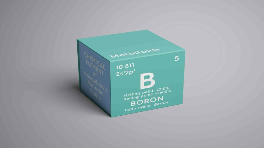
Boron and graphene are two materials that have immense potential in the field of electronics. Boron is a naturally occurring element, with atom number 5 in its periodic table column (group III-A). At the same time, graphene has magnetic properties as an allotrope of carbon consisting solely of sp2 bonded atoms.
The infinite possibilities for boron’s use stem mainly from it being able to be found easily at low costs due to how common it is on earth; this material can also exhibit unique electrical characteristics because it conducts electricity much as metals do but without differentiating between positive or negative charges – unlike most semiconductors which only pass electrons through one way, thus making them ideal candidates for creating transistors.
According to some recent studies, it has been found out that low-energy Boron ion implantation in Graphene can significantly improve its electrical qualities that can be further used for many applications. The use of molecular dynamics simulations and adaptive bond order calculations to bombard boron and nitrogen ions at a 70° oblique angle can improve productivity by over 25%.
Boron and Silicon
They are crucial for Silicon’s growth and form an excellent boron-silicon interface, an excellent semiconductor material. Boron interacts with silicon through covalent bonds. The resulting change in energy levels can significantly affect physical properties such as thermal conductivity, ionic conduction bandwidths, electrical resistivities etc.
An example: One study that researchers from Purdue University conducted showed how Boron ions could improve electron mobility within Graphene sheets after irradiation at low energies (40 keV). Boron can form solid chemical bonds with Silicon during its formation process, making it one of the most popular materials used in various technological applications today.
Boron-doped silicon can also be used as a replacement for the more expensive germanium. Boron doped silicon has been proven to have better performance than pure crystalline low-cost materials such as Germanium, and it’s easy enough o produce on large scales with conventional deposition processes from silane gas mixtures at temperatures below 1000°C.
Boron Carbon Nitride and the future of nanoelectronics
BCN materials are attracting attention for their varied applications, which have proven advantageous in the harshest environments. The BCN material is recognised for its adaptable electrical properties and outstanding mechanical behaviour, making it perfect for corresponding applications where extreme conditions dominate.
Boron carbon nitride (BCN) compounds are known to combine the properties of B4C and h-BN depending on their composition, making them an excellent semiconductor. BCN is formed between graphite and h-BN, with its output tone being adjustable based on this combination. A semimetallic material containing nitrogen atoms that can either be in sp3 or sp2 hybridisation has one less bandgap than graphene, making it highly conductive at low temperatures when electrons are confined within these bands.
Initially, BCN Compounds were sought after for their dielectric properties and subsequently became the focus of semiconductor development. Boron solutions have been shown to clean areas of graphene that accumulate undesired charges, which may lead to imperfections and voids on the surface, making it less conductive and more challenging to produce with high yields.
Boron materials are also being researched for radiation hardening effects where borons are implanted into semiconductors through an irradiation process during their manufacture. This decreases leakage current by up to ten times while increasing carrier lifetime at room temperature.
Introduction to nanomaterials
Nanomaterials, although they currently only exist in the lab and haven’t been produced in large quantities to be used by humans regularly yet, will soon take an essential role as we look for ways to make our world cleaner. These nanoscale materials are so small that it’s hard even to see them with conventional microscopes – imagine what their effects might do!
Nanotechnology is still relatively new but has already had profound implications on many aspects of life due to its ability to create objects at scales far too minuscule for human beings or machines using ordinary means. The potential applications include medicine (diagnosis and treatment), environmentally friendly products such as paints that can clean themselves without harsh chemicals), electronics manufacturing processes where reasonable quality control would be much easier than today’s methods.
The world needs new technologies to solve its increasing environmental issues. Developing nanomaterials with desirable tunable properties has been challenging, and it continues to be so as the demand for these materials only grows higher. One of the reasons for this is that many materials behave in a certain way under specific conditions, and it has not been possible to control their properties at will. Boron-doped silicon nanowires exhibited good results as an alternative material with tunable optical properties – they were able to produce light within a broad range of wavelengths by being stimulated by different types of external stimuli such as heat or electrical stimulation.
BCN and its electrical properties
BCN hybrid materials exhibit impressive electrical properties due to their exclusive phase in the B–C–N ternary triangle. Additionally, the flexibility of fine-tuning the properties based on elemental film composition to satisfy specific requirements makes BCN films lucrative for electrical applications. Metal–insulator metal (MIM) devices are commonly fabricated to perform I−V and C−V measurements of the material when it is used as an insulator or a conductor depending on how they’re situated within their application with other compounds such as silicon dioxide substrate layers that create semiconductors.
Conclusion
Boron and its compounds have far reaching implications in the world of electronics. Both – graphene and nanoelectronics – will be essential in building the technology of tomorrow. Graphene is already being used in every industry, from rockets, automobiles, and even graphene-based batteries that can last a longer time as compared to lithium batteries. Similarly, it is said that nanoelectronics will revolutionise the field of medicine and computing.
As the world continues to rely more on electronics, it is important for everyone to be aware of Boron. It can serve as a component in graphene and nanoelectronics, but also has its uses elsewhere in various fields such as medicine and aerospace engineering. As we continue our journey into an increasingly electronic future with innovations coming out every day – Boron will always have its place.


